Advanced and legacy processes are improved by this next-generation material having superior gapfilling and planarizing capabilities and simplified, defect-free, and extremely clean removal.
Rolla, MO – February 8, 2023 – Brewer Science, Inc., a global leader in developing and manufacturing next-generation materials for the microelectronics and optoelectronics industries, announces the launch of OptiStack® PL200 series material, a silicon-rich high-aspect ratio gapfill material designed to provide superior planarization, solving problems faced in sacrificial gapfill applications. This material series also facilitates next-generation advanced-node patterning by providing a protective, easily strippable, gapfill material that overcomes challenges with nanosheet architectures.
Gapfill for <10-nm trenches is necessary to achieve advanced node patterning
OptiStack® PL200 series material is an innovative spin-on, silicon-rich gapfill material providing extremely low defectivity in comparison to legacy gapfill materials. This material series is designed to provide excellent gapfill of <10-nm trench and via structures, while also providing superior planarization for robust, faithful lithography and etch transfer. The stability of the product provides a long shelf life of 365 days (at 21°C).
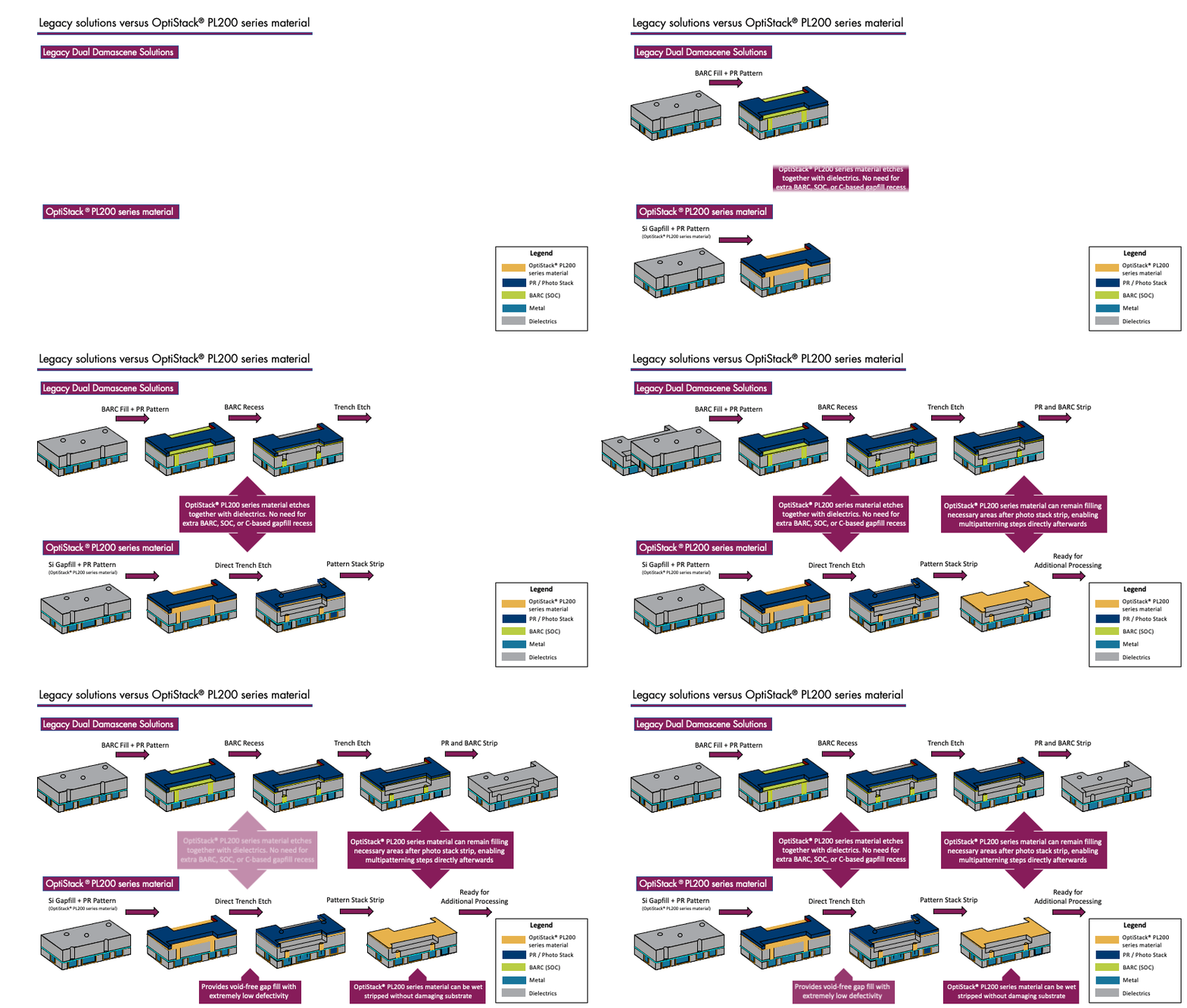
The following simplified example illustrates one potential use of OptiStack® PL200 series material to improve a Dual Damascene process:
Dual damascene is an important process in all modern back end-of-line (BEOL) metallization to make copper interconnects. One critical step during dual damascene is gapfilling the incoming via structures to prepare for subsequent trench opening. Traditionally, a thick bottom antireflective coating (BARC) or organic gapfill material was used to fill the vias. Because some of the lower metal layers now must go through multiple patterning steps to achieve the required critical dimensions (CDs), the whole gapfill, patterning, and etching process becomes even more complicated.
The new OptiStack® PL200 series material improves the traditional process in several ways:
- Fewer steps. The ability to match oxide etch rates. Because the new material etches together with surrounding dielectric materials, the extra recess step needed when a traditional SOC gapfill is used can be eliminated.
- More compatible with pitch splitting processes. The new material has very low shrinkage in O2 based ash processes. It can survive the photoresist stripping and be ready for the subsequent 2nd and 3rd photo steps for multiple patterning.
- Easy to strip. OptiStack® PL200 series material is completely removable by several common wet etch chemistries, such as SC1. The single-step, wet clean with zero defect capability also helps in next-generation applications by providing an effective clean for narrow, horizontal nanosheets.
- CMP compatibility. When a strict global-level planarization is needed, this new material can be further planarized by CMP for use in high topography, and/or highly variable pattern density devices.
Compared to legacy solutions, OptiStack® PL200 series material offers unparalleled gapfilling capability, superior planarity over various pitch densities, extremely low shrinkage in O2 ash, and minimal defectivity, all essential in yield improvement for many fabrication layers in advanced nodes.
OptiStack® PL200 series material shows great potential in other applications, especially in advanced Fin-FET processes and future architectures, such as forksheets, nanosheet/gate-all-around (GAA) and CFET.
“Advanced logic and foundry platform technologies require a high-aspect ratio gapfilling material that protects structures and easily strips without residue,” states Jim Lamb, Corporate Fellow at Brewer Science. “OptiStack® PL200 series material meets this need.”
Reduces yield loss from inadequate cleaning in advanced processes
A traditional plasma cleaning process is insufficient at cleaning deep structures, leading to potential contamination or damage to transistor structures. In forksheet, or nanosheets/gate-all-around transistor structures, cleaning of the horizontal nanosheets is crucial because residual material on or between nanosheets can prevent removal, or deposition, of subsequent atomic layers. A cleaning with SC1 effectively removes OptiStack® PL200 series material and does not damage critical areas when building the N-type metal oxide semiconductor (NMOS) and p-channel metal-oxide semiconductor (PMOS) structures.
To learn more about OptiStack® PL200 series material, please visit Brewer Science’s Advanced Lithography Materials webpage, and submit a request at the bottom of the page to connect with a product expert.
About Brewer Science
Brewer Science is a global leader in developing and manufacturing next-generation materials and processes that foster the technology needed for tomorrow. Since 1981, we’ve expanded our technology portfolio within advanced lithography, advanced packaging, smart devices, and printed electronics to enable cutting-edge microdevices and unique monitoring systems for industrial, environmental, and air applications. Our relationship-focused approach provides outcomes that facilitate and deliver critical information. Our headquarters are in Rolla, Missouri, with customer support throughout the world. We invite you to learn more about Brewer Science at www.brewerscience.com.
###
Company Contact:
Nathan Ayres
Tel: (US) +1.573.364.0300, ext. 1923
Email: nayres@brewerscience.com


