Brewer Science lithography products have been shaping the semiconductor industry since 1981. Over the years, new product lines, capabilities, and specifications have been improved to deliver the best performance to our customers. Focusing on improving quality and manufacturing efficiencies, we have become the go-to supplier of next-generation lithography materials.
Anti-reflective Coatings the original bottom anti-reflective coatings (BARCs), ARC® anti-reflective coatings continue to be the industry benchmark for reflection control and light absorption during photolithography.
Multilayer Systems used in combination with our proprietary OptiStack® optical modeling system to achieve the finest resolutions possible with 193-nm immersion lithography.
EUV assist underlayers that enable faster development of EUV photoresist and processes
Brewer Science has put the resources and investments into manufacturing that are necessary to reach and achieve our customers’ goals. Our numerous cleanroom environments down to Class 10 help provide the cleanest and purest environments for manufacturing. Within these cleanrooms, we have built closed-loop systems utilizing state-of-the-art software for automating and monitoring our processes.
The investments to our product improvements didn’t just stop at manufacturing product but continue into our quality control, quality engineering, analytical, and applications groups as well. Over the years we have improved the testing of our materials down to 1-part-per-trillion (1 ppt) and are working to achieve 1-part-per-quadrillion (1 ppq) results. To do this we use, and continue to invest in, leading edge analytical and process equipment.
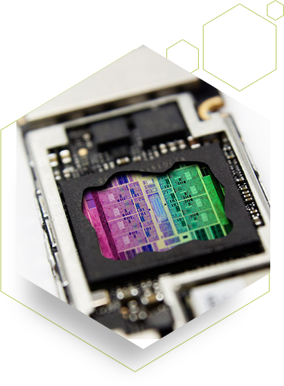
All the amazing advances in the electronics age have been enabled by Moore’s Law. This law of continual miniaturization of integrated circuits is directly driven by the technology that determines the size and density of the patterns we can create through advanced photolithography.
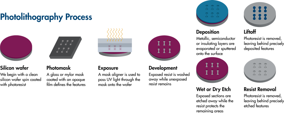
Photolithography is the process of using light to transfer geometric patterns from a photomask to light-sensitive chemicals on a substrate. These patterns are what make up the electrical circuitry of every semiconductor device. This process usually consists of a series of chemical depositions, patterned exposures, and selective removals to produce the required features on the substrate layer by layer.
Although the speed of Moore’s Law is slowing down, there is still a future for lithography within front-end chip processing. New materials will need to be able to withstand higher temperature processing to be compatible with chemical vapor deposition (CVD) layers for stacking.
Brewer Science is at this forefront of innovation for next generation materials to help continue front-end processing for the foreseeable future.
| ARC® | Multilayer | EUV |
Advanced Lithography
