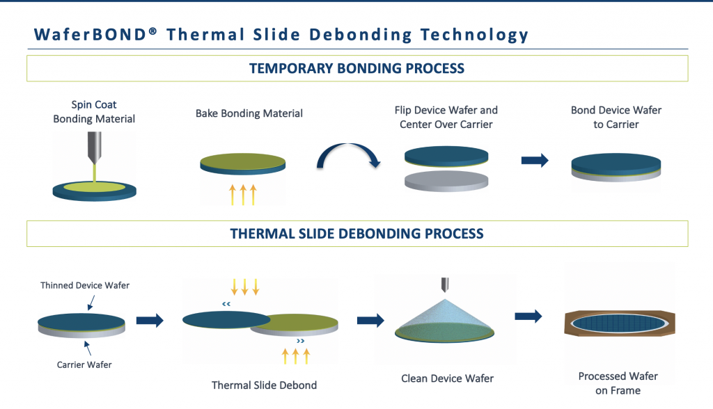
WaferBOND® HT-10.11 temporary bonding material enables back-end-of-line (BEOL) processing of ultrathin wafers with standard semiconductor equipment.
WaferBOND® HT-10.11 material is an organic coating developed for temporary wafer bonding solutions for MEMS and 3-D wafer-level packaging applications. WaferBOND® HT-10.11 material enables effective bonding and support through substrate thinning and backside standard lithographic processing through the utilization of effective bonding and subsequent thermal slide, chemical*, mechanical**, or laser** debonding for thickness < 75 μm. These materials were specifically developed for thin wafer handling (TWH), through-silicon via (TSV) reveal, and redistribution layer (RDL) creation or processes up to 250°C.
*Chemical release debond method requires a perforated carrier wafer or small die size if releasing after dicing
**Mechanical and laser debond methods require a compatible release material
WaferBOND® HT-10.11 material is an organic coating that enable back-end-of-line (BEOL) processing of ultrathin wafers using standard semiconductor equipment. This material is a great option as an alternative solution to typical wax adhesives. WaferBOND® HT-10.11 material offers significant advantages because it can be applied with a one-coat process, improve throughput, simplify cleaning, and shorten processing time.
| Properties | Wax | WaferBOND® HT-10.11 Material |
|---|---|---|
| Thickness Range | ~ 10 – 35 µm | 20 µm – 130 µm |
| Coating Throughput | Requires multiple coats | Single-coat process |
| Bonding Temperature Range | 95°C – 110°C | 130°C – 180°C |
| Debonding Temperature Range | 95°C – 110°C | 150°C – 200°C |
| Thermal Stability Temperature Range | < 120°C | ≤ 250°C |
WaferBOND® HT-10.11 material is compatible with the following debond methods:
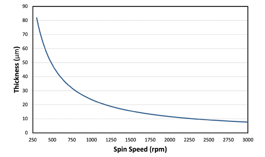
WaferBOND® HT-10.11 Material Spin Speed Curve:
WaferBOND® HT-10.11 Material