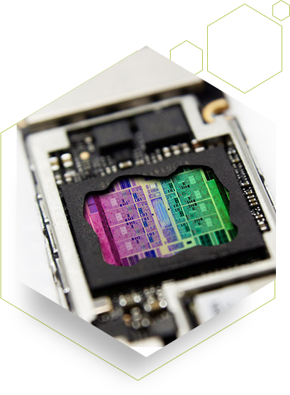
在每个智能手机、平板电脑和笔记本电脑内
都有大量集成电路 - 这些小黑正方形和矩形是一个设备的心脏、灵魂和大脑。您看到的不是芯片本身,而是绝缘并保护芯片内层的黑色环氧树脂封装。芯片通常是包含数百万微型电子元件和连接件的小型薄硅片。
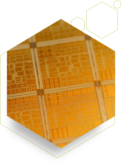
在芯片封装和
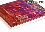
 集成至您的电子设备之前,每一个都是在被称为晶圆的更大的硅片上的单个芯片。在晶圆表面上建立集成电路需要数百个步骤,其中许多步骤涉及使用光将复杂电路图案转移到光敏涂层中。这个工艺被称为 光刻法,并且它是制造微小集成电路过程中最关键也是最具挑战性的步骤之一。
面临的一个挑战是
硅片是有光泽的,并且会反射用于在表面上产生微电路图案的光。芯片制造商必须找到一种方法管理在进行光刻期间晶圆产生的反射。
这就是我们切入的地方。
控制光。改变世界。
Brewer Science has been developing cutting-edge materials and processes for controlling light during photolithography for over four decades. 如果没有 ARC® 抗反射涂层,电子产品不会像今天这般小巧、快速并且价格低廉
我们没有停止探索。
控制光不是 Brewer Science 的唯一闪光点。With over 40 years of experience in materials research, we are constantly looking for new ways to move technology forward. A few other areas where we are making waves include 3-D stacking of integrated circuits and smart devices & printed electronics.
![]()
