Imec and Brewer Science present process solutions for CVD oxide deposition processes on ultrathin wafers at Electronic Components and Technology Conference (ECTC)
Process challenges during CVD oxide deposition on the backside of 20-µm thin 300-mm wafers temporarily bonded to glass carriers
Grande Lakes, FL – May 22, 2023 – Brewer Science, Inc., a global leader in developing and manufacturing next-generation materials and processes for the microelectronics and optoelectronics industries, is presenting and exhibiting at Electronic Components and Technology Conference (ECTC) May 30th through June 2nd.
Dr. Koen Kennes from imec is copresenting with Brewer Science, Process challenges during CVD oxide deposition on the backside of 20-µm thin 300-mm wafers temporarily bonded to glass carriers, which evaluates a temporary carrier system during several backside processing steps on thin wafers down to 20 µm. The main focus is the impact of various chemical vapor deposited (CVD) oxides on thinned wafers supported by temporary bonding materials. Such wafers have the risk of deformation and even delamination during the deposition step. The presentation is May 31st at 10am, a part of Session 37: Interactive Presentations.
A step-by-step investigation reveals the deformation/delamination mechanism to be highly dependent on the oxide deposition conditions rather than the deposition temperatures. Controlling the stress in the oxide layer enables both high-temperature and low-temperature oxides to be successfully deposited on the backside of ultrathin wafers. The experimental results are corroborated with finite element simulations.
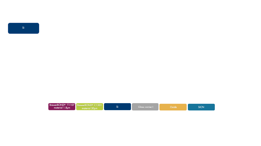
Figure 1. Schematic of the process flow. The wafer thinning starts by edge trimming the wafer followed by coating the release layer, BrewerBOND® T1107 material. After bonding with the temporary bonding material (TBM), BrewerBOND® C1301-50 material, the wafers are ground down to 55 µm and chemical mechanical polished (CMP) to smooth the surface. Further thinning is achieved via a wet etch step. After oxide and dielectric deposition, several wafers are transferred to a new carrier using a wafer flip step in which the original stack is bonded to a second carrier enabling debond of the first carrier.
“During high-temperature CVD oxide deposition on thinned wafers on temporary carriers, delamination of the thin wafer from the carrier was observed.” States Dr. Kennes, R&D team lead for bonding, assembly, and wafer-level packaging at imec. “Using FEM simulations and DOE experiments, the failure mechanism was identified, and process solutions were defined. This resulted in successful damascene processing on the backside of thinned wafers on glass carriers.”
Brewer Science is a Gold Sponsor of ECTC. You can connect with Brewer Science at booth #110 throughout the duration of the event May 30th through June 2nd. Learn more about Brewer Science’s innovative packaging solutions on their website, and connect with an expert by submitting a request on their website.
About Brewer Science
Brewer Science is a global leader in developing and manufacturing next-generation materials and processes that foster the technology needed for tomorrow. Since 1981, we’ve expanded our technology portfolio within advanced lithography, advanced packaging, smart devices, and printed electronics to enable cutting-edge microdevices and unique monitoring systems for industrial, environmental, and air applications. Our relationship-focused approach provides outcomes that facilitate and deliver critical information. Our headquarters are in Rolla, Missouri, with customer support throughout the world. We invite you to learn more about Brewer Science at www.brewerscience.com.
###
Company Contact:
Nathan Ayres
Tel: (US) +1.573.364.0300, ext. 1923
Email: nayres@brewerscience.com